
“[A] large amount of the federal funding appropriated under the CHIPS and Science Act has already been allocated to some of the biggest names in the chip manufacturing industry.”
 On April 16, the U.S. Department of Commerce announced that the Biden Administration had issued a notice of funding opportunity (NOFO) earmarking $54 million in funds available under the CHIPS and Science Act to fund advances in measurement technologies critical to semiconductor production. These funds, administered via grant through the Small Business Innovation Research (SBIR) program, are expected to improve U.S. leadership in computer chip manufacturing by mitigating production defects and increasing production yields.
Funds Administered by NIST to Address Seven Challenges in Measurement Science
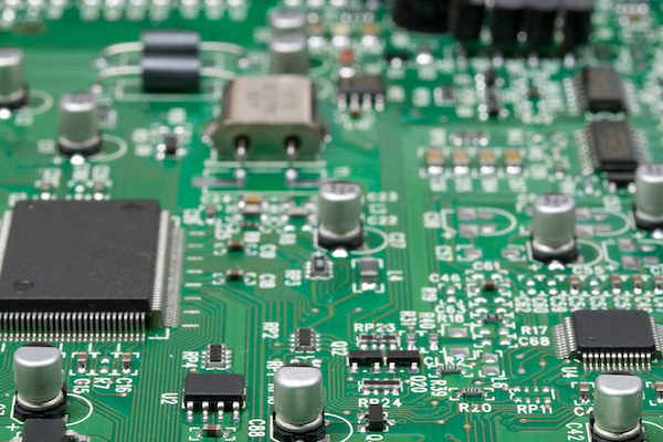
In August 2022, the same month that President Joe Biden signed the CHIPS and Science Act into law, the National Institute of Standards and Technology (NIST) issued a report outlining seven major challenges in semiconductor metrology, which involves the application of measurement science to ensure that advanced multi-layered computing chips are manufactured without defect across hundreds of manufacturing steps. Then, in June 2023, NIST issued another report detailing metrology gaps in the semiconductor ecosystem, identifying a series of 10 priority focus areas in supply chain assurance, interoperability standards, and metrology for nanostructured materials and 3D structures.
The recent NOFO from the Biden Administration seeks applications from small businesses that are developing products or services that they expect to commercialize in the microelectronics marketplace. Specifically, SBIR grant funding will be awarded to companies providing breakthrough advances in material characterization, instrumentation, testing and manufacturing capabilities. NIST, which is administering the SBIR funding program, has indicated that it will be seeking to fund projects that advance U.S. leadership in metrology standards, deploy innovative manufacturing metrologies, develop provenance technologies and establish research and development (R&D) testbeds for metrology.
The research areas eligible to apply for funding under the Biden Administration’s recent NOFO correspond to the seven challenges identified in the August 2022 NIST report. To better model and simulate semiconductor materials, designs and components, CHIPS and Science Act funding through the metrology program will be awarded for critical R&D in multi-physics models as well as machine learning and artificial intelligence technologies for modeling complex circuits operating in real environments. Projects enhancing the security and provenance of microelectronic-based components are eligible for funding if they enhance vulnerability management across the product lifecycle. Funds will also be earmarked for advanced metrology projects in physical properties characterization, non-destructive techniques for characterizing defects and impurities, and evaluation of relevant data across the semiconductor manufacturing process.
CHIPS and Science Act’s $39 Billion for Onshore Production Will Be Allocated This Year
While the recent NOFO targets semiconductor metrology projects being developed by small businesses, a large amount of the federal funding appropriated under the CHIPS and Science Act has already been allocated to some of the biggest names in the chip manufacturing industry. In late March, the Commerce Department announced that it had entered into a memorandum of understanding with Intel Corporation that makes the American semiconductor giant eligible for nearly $20 billion in funding, with $8.5 billion of that coming directly from CHIPS and Science Act funding, in exchange for commitments to build or modernize several chip fabrication facilities across the United States.
Federal appropriations for semiconductor funding are also being used to attract investments from chipmaking leaders situated overseas. One week before the Biden Administration released the NOFO for metrology projects, Taiwan Semiconductor Manufacturing Corporation (TSMC) announced that it was eligible for up to $11 billion in funding, including $6.6 in direct funds, to expand chip fabrication construction projects in the area of Phoenix, AZ. Then one day prior to the NOFO, South Korean conglomerate Samsung announced that it will be receiving $6.4 billion in CHIPS and Science Act funding to support corporate investments of more than $40 billion into semiconductor manufacturing plants in Taylor, TX, a suburb of the state’s capital city of Austin. The same day the funding for Samsung was announced, Commerce Secretary Gina Raimondo made public comments indicating that the $39 billion earmarked under the CHIPS and Science Act to build U.S. domestic semiconductor facilities would be allocated by the end of this year.
Image Source: Deposit Photos
Author: Alekcey
Image ID: 1696588
![[Advertisement]](https://ipwatchdog.com/wp-content/uploads/2024/04/UnitedLex-May-2-2024-sidebar-700x500-1.jpg)
![[Advertisement]](https://ipwatchdog.com/wp-content/uploads/2024/04/Patent-Litigation-Masters-2024-sidebar-700x500-1.jpg)

![[Advertisement]](https://ipwatchdog.com/wp-content/uploads/2021/12/WEBINAR-336-x-280-px.png)
![[Advertisement]](https://ipwatchdog.com/wp-content/uploads/2021/12/2021-Patent-Practice-on-Demand-recorded-Feb-2021-336-x-280.jpg)
![[Advertisement]](https://ipwatchdog.com/wp-content/uploads/2021/12/Ad-4-The-Invent-Patent-System™.png)


Join the Discussion
No comments yet. Add my comment.
Add Comment