
“Samsung” by Samuel T. Livingston. Licensed under CC BY 2.0.
Seoul, South Korea-based Samsung Electronics (KRX:005930) is a consumer electronics developer which has made its presence felt in the mobile computing device sector, which includes smartphones, tablets and wearables. There have been media reports that the tech firm will release a foldable smartphone with an organic light-emitting diode (OLED) screen sometime next year. This company’s tech developments often put it at odds with consumer electronics designer Apple Inc. (NASDAQ:AAPL) and reports of Samsung announcement that it’s developing an electric car opens up another front on which the two firms can compete. It’s possible that this car could feature a smart windshield like the one developed by Samsung in partnership with Japanese motorized product developer Yamaha (TYO:7272). Although the narrative surrounding these two companies revolves around their rivalry in the smartphone wars, Samsung recently helped Apple escape at least some patent infringement damages by filing a covered business method (CBM) review at the Patent Trial and Appeal Board (PTAB); the CBM successfully struck down claims which had been used to allege infringement against both Samsung and Apple.
In mobile news, Samsung is the latest tech company which will be offering its electronic wallet products in China, where it competes in that sector against Apple and Chinese e-commerce company Alibaba Group (NYSE:BABA). In virtual reality tech, Samsung has collaborated with Spanish mobile phone operator Movistar to broadcast a live feed of a soccer match between Real Madrid and 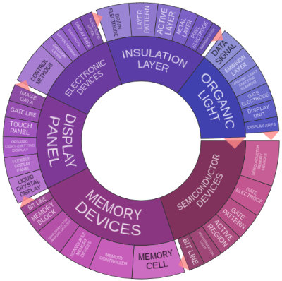 Barcelona in early April on Samsung’s Gear VR platform. Highlighting the widespread pursuits of the entire Samsung Group is the recent news that the conglomerate’s drug development arm has produced a generic arthritis drug which is approaching successful regulatory approval in Europe.
This company has attained a solid second-place position in the U.S. patent world behind perennial first-place finisher IBM (NYSE:IBM). In 2015, Samsung Electronics earned a total of 5,072 patents from the U.S. Patent and Trademark Office, a slight increase from the 4,936 U.S. patents which the company took home in 2014. Including design and utility patents, Samsung has already taken in 2,017 U.S. patents since the beginning of 2016, an incredible pace which would blow past the firm’s 2015 totals if it holds up all year. As the text cluster from Innography shows us here, much of this recent research and development has focused on semiconductor devices, memory devices and display panels.
![[[Advertisement]]](https://ipwatchdog.com/wp-content/uploads/2024/04/Patent-Litigation-Masters-2024-banner-early-bird-ends-Apr-21-last-chance-938x313-1.jpeg)
Samsung’s Issued Patents: From Folding Device Screens to Antibody Screening Methods
 We were able to find a Samsung patent related to foldable screens used in display devices, reflected within U.S. Patent No. 9287341, which is titled Flexible Display Device Including Folding Section. It protects a flexible display device having a folding section formed on a flexible substrate, a flat section connected to the folding section and a display area formed on the folding section and the flat section, the display area having pixels and a plurality of wires supplying electrical signals to the pixels, one of which is a winding wire extending in a winding configuration. This innovation improves a flexible display device’s ability to withstand the forces of compressive and tensile stresses generated from repeated folding.
Wearable devices providing enhanced sensory feedback are at the center of U.S. Patent No. 9286774, which is titled Tactile Sensation Providing Apparatus. The apparatus claimed here includes a tactile output unit comprising a contact surface to contact a part of a human body, a body portion and a first frame to which the body portion is slidably mounted to guide the body portion horizontally; the apparatus also includes a connection unit with a wire connected to the tactile output unit, a tube enclosing the wire and a driver supplying a driving force to the connection unit. This device could provide a range of tactile sensation feedback, including oscillations, heat or force.
Energy efficiency in high speed data transmissions is better achieved thanks to the innovation outlined within U.S. Patent No. 9294382, titled Communication Device and Method for Enhancing Energy Efficiency. It discloses a method for increasing energy efficiency of a communication device by adaptively determining a clipping ratio of a signal input based on a modulation scheme of the communication device, performing an inverse fast Fourier transform (IFFT) on the input signal and clipping the IFFT signal based on the determined clipping ratio wherein the ratio is higher as a maximum allowable single amplitude increases and lower as a power of the input signal increases. This invention addresses a need for increasing power efficiency in communication devices without the link interference caused by high dimensional modulation.
 The use of computing devices to improve an individual’s ability to socialize through telecommunications is discussed within U.S. Patent No. 9294429, which is titled Method and System for Providing Service for Searching Friends. It protects a method of providing a friend search service of a terminal which involves transmitting a message for controlling a microphone of a second terminal of a server, outputting a sound including a first encryption key after transmitting the message, receiving a second encryption key from the second terminal through the network, checking second terminals existing in a sound-reaching area by comparing both encryption keys and displaying a friends list including the second terminals existing in the sound-reaching area. This technology improves on conventional location-based friend search services by providing a means by which they can check on the locations of friends adjacent to each other.
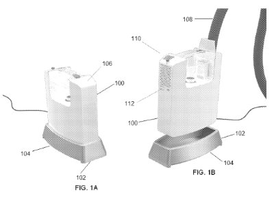 Home appliances still constitute an important area of Samsung R&D, as is evidenced by the issue of U.S. Patent No. 9282858, which is titled Portable Vacuum with a Charging Base and Dustpan Mode. It discloses a vacuum cleaner system having a vacuum body with an internal dust collector component and a charging base having a dirt inlet at its bottom so that the vacuum force created by the vacuum body is collected through the charging base’s dirt inlet and remains in the internal dust collector component. This innovation is designed to merge the convenience of using portable cleaners for cars and other small spaces with the cleaning force of a full-size upright vacuum.
Patent Applications of Note: More Flexible Displays and Grip Sensing for Devices
We found more technologies related to folding electronic displays in our survey of Samsung’s patent applications, such as the one described in U.S. Patent Application No. 20160085369, filed under the title Foldable Display. It claims a foldable display having a single bendable display substrate, a data driver detachably connected to the display substrate and a controller unit that controls the data driver; the display substrate includes a substrate body, a display element on a first surface, a pad unit on another surface and a transparency adjusting layer. This configuration is designed to enable a folding display which can support a large sized screen. Other  types of flexible display devices are at the center of U.S. Patent Application No. 20160079329, which is titled Rollable Display Device. This would protect a rollable display device having a roll frame and a flexible display unit windable in the roll frame, the flexible display unit having a flexible substrate, a display layer on the flexible substrate, an encapsulation layer that seals the display layer, a polarization layer, a touch screen layer and a protection layer sequentially disposed on the encapsulation layer. This innovation is designed to again reduce the stress imparted to such flexible screens when they are rolled up.
Augmented and virtual realities have been in focus since VR took center stage at this year’s Consumer Electronics Show and we took note of a Samsung innovation in this field, reflected within U.S. Patent Application No. 20160077335, which is titled Optical Device for Augmented Reality. The optical device for augmented reality claimed here has a light input part having a micro display, a first polarizing beam splitter, a second polarizing beam splitter that reflects or transmits incident light of an image displayed on a micro display and a first quarter wavelength plate that receives light transmitted by either polarizing beam splitter and change a polarized state of a received light; the light output part includes a third polarizing beam splitter, a fourth polarizing beam splitter transmitting or reflecting received from the light input part, a second quarter wavelength plate receiving light from the third or fourth splitter and a light condenser that condenses the polarized light. The incorporation of beam splitters and other components in this invention results in the ability to provide augmented reality services through an optical device of a reduced thickness.
Samsung is involved in the world of medical diagnostics research as our readers can tell from the filing of U.S. Patent Application No. 20160093046, entitled Apparatus and Method for Supporting Computer Aided Diagnosis. It would protect an apparatus having a control processor that determines a duration during which a remaining image of a first region of interest (ROI) detected from a first image frame is displayed and then a display that marks a remaining image of a second ROI of a second image frame in the first image frame and display the marked image on a screen. This invention addresses a shortcoming in convention computer aided diagnostic systems used in healthcare settings by which medical issues could be missed if the region of interest is too small or a technician moves a probe over the region of interest too quickly.
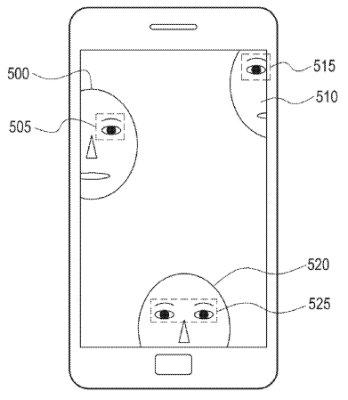 Facial recognition technologies increasing the ease of inputting function commands into a computer are discussed within U.S. Patent Application No. 20160085496, titled Apparatus and Method of Controlling Mobile Terminal Based on Analysis of User’s Face. The apparatus claimed here includes a display, a camera configured to capture an image for a user and a processor that performs face detection on the image, performs eye detection on the image if the face detection fails and control the display to be maintained in a turn-on state based on face detection results or eye detection results. This facial recognition technology is designed for mobile devices and improves recognition when the face is partially obscured or presented to the camera at an improper angle. Other new types of input to perform commands on portable electronic devices are also described within U.S. Patent Application No. 20160076952, which is titled Electronic Device and Grip Sensing Method. This would protect an electronic device having a display, a housing including a front display surface, a rear surface and a side surface, a wireless communication module in the housing, at least one antenna pattern electrically connected to the wireless communication module and forming an electromagnetic or magnetic field, a detection circuit electrically connected to the antenna pattern for detecting a current and/or voltage associated with the antenna pattern and a processor connected to the wireless communication module and the detection circuit to change part of an operation of a wireless device in response to a detected current and/or voltage change. This innovation enables electronic devices to incorporate grip inputs into the list of input commands which can be performed by device users without the added expense of an additional grip sensor.
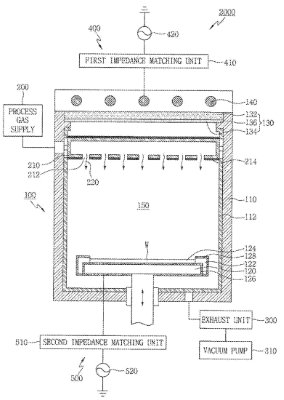 Finally, we took a close look at a Samsung technology for the increased yield of semiconductors in fabrication processes which is outlined within U.S. Patent Application No. 20160079040, entitled Plasma Processing Devices Having a Surface Protection Layer. The plasma processing device that would be protected here includes a process chamber body, a substrate support unit in a lower portion of the process chamber body, a window part in an upper portion of the process chamber body and a surface protection layer on the window part’s base layer which is comprised of an oxide having a columnar structure. This invention is designed to reduce the damage sustained by the window part when generating high density plasma, which can damage a plasma processing device and create particles which reduce the device’s lifetime.
![[Advertisement]](https://ipwatchdog.com/wp-content/uploads/2024/04/Patent-Litigation-Masters-2024-sidebar-early-bird-ends-Apr-21-last-chance-700x500-1.jpg)

![[Advertisement]](https://ipwatchdog.com/wp-content/uploads/2021/12/WEBINAR-336-x-280-px.png)
![[Advertisement]](https://ipwatchdog.com/wp-content/uploads/2021/12/2021-Patent-Practice-on-Demand-recorded-Feb-2021-336-x-280.jpg)
![[Advertisement]](https://ipwatchdog.com/wp-content/uploads/2021/12/Ad-4-The-Invent-Patent-System™.png)


Join the Discussion
No comments yet.